MSXB 042: Input Termination for the iDSC 1816
Technical Note TN-225: Version 1.00
The Microstar Laboratories Input Termination Board, part number MSXB 042, is a 32-point quick-connect termination board for the input connector on the iDSC board. The MSXB 042 provides a ground connection for each input signal and each output signal, allowing easy connection to discrete devices.
All input connections are labeled with both the signal name and the pin number of the 50-pin connector on the iDSC board.
Note: The MSXB 042 should not be connected or disconnected while the iDSC board is powered.
Analog Inputs
The analog inputs of the MSXB 042 come from the factory configured for voltage input. The inputs can be configured for current input or for input voltages that exceed iDSC board specifications.
Current Input
To configure a current input, place a resistor in the location on the termination board corresponding to the input pin being reconfigured. Figure 1 and Table 1 show resistor placement. The appropriate size for this resistor can be calculated using Ohms law, given the maximum input current and the input voltage range of the iDSC board.
Ohm's Law: Resistance = Voltage / Current
The iDSC board is shipped from the factory with an input range of +/- 5 volts. The accuracy of the measurements made in this configuration depends on the precision of the resistors used and this should be taken into consideration when selecting the resistors. Microstar Laboratories recommends using resistors with a 1% or better tolerance.
Excess power dissipated in the resistor causes heating; this changes the resistance value, decreasing the accuracy of the measurements. The recommended maximum power dissipation is 0.1 watt.
Power Calculation: Power = current2 * resistance
For current input, a current source is connected to the Ax+ terminal and the ground return is connected to the Ax- terminal. To convert voltage input A0 into a current input that generates 1 to 5 volts with an input current of 4 to 20 milliamps, a 250 ohm resistor is inserted in the R15 location. In this case, the maximum power dissipated in the resistor is 0.1 watt at +5 volts; this is the maximum recommended power dissipation. Figure 1 illustrates the connections for this example.
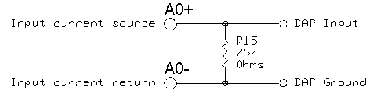
Figure 1
Voltage Divider
The termination board can be configured for applications requiring input voltages greater than that allowed by the iDSC board. This is accomplished by soldering a resistive voltage divider in the location provided on the termination board. Before this can be done, a trace on the termination board must be cut. Above each even numbered resistor there is a row of five small holes. Between two of the holes there is a white "X". The trace at the X must be cut.
Once this trace is cut, the resistors for the voltage divider are soldered into place. The resistor on the ground side of the divider is placed in an odd numbered resistor location and the resistor on the input signal side of the divider is placed in an even numbered resistor location. Figure 2 and Table 1 illustrate resistor placement for each input.
After both resistors are soldered into place, signals may be connected between the Ax+ and Ax- terminals. Test the voltage divider circuit before connecting the circuit to the iDSC board.
Note: Be careful to avoid applying an input voltage that exceeds iDSC board specifications.
Warning: If the trace on the termination board is not cut, the high voltage input is connected directly to the iDSC board input; this may damage or even destroy the iDSC board.
For example, to configure input A0 so that an input range of 0 to 20 volts is scaled down to a range of 0 to 5 volts, a resistor ratio of 3:1 is needed.
Voltage Divider Equation: Vout= Vin* R1/(R1+R2)
Resistance values of 1500 and 500 ohms may be used. The trace beneath the X above R16 is cut. Then the 500 ohm resistor is placed in the R15 position and the 1500 ohm resistor is placed in the R16 position. Since 500 ohm resistors are not commonly available, a 510 ohm resistor would typically be used instead, resulting in a small error in the division ratio. This error is linear and can be corrected by multiplying by a constant in DAPL. Figure 2 illustrates the circuit for this example.
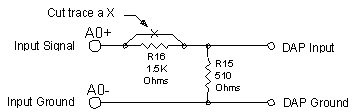
Figure 2
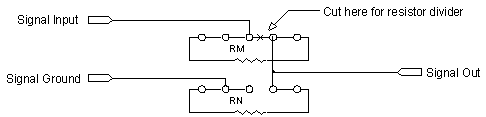
Figure 3
Note: To avoid exceeding iDSC board input voltage specifications, make sure both resistors are securely soldered in the correct locations and the trace beneath the X is completely cut before using the circuit.
| Terminal | Current Input Resistor* | Voltage Divider Resistors** |
|---|---|---|
| A0+, A0- | R15 | R15, R16 |
| A1+, A1- | R13 | R13, R14 |
| A2+, A2- | R11 | R11, R12 |
| A3+, A3- | R9 | R9, R10 |
| A4+, A4- | R7 | R7, R8 |
| A5+, A5- | R5 | R5, R6 |
| A6+, A6- | R3 | R3, R4 |
| A7+, A7- | R1 | R1, R2 |
* The current input resistor is placed in the ** The first resistor is on the ground side of the voltage divider ( |
||
Table 1 and Figure 3 can be used to locate the appropriate resistors when using either the current input or voltage division configuration. Figure 3 shows schematically how the inputs and grounds on the termination board are connected.
Control Lines
The Input Termination Board has connections to iDSC board external timing channels. The connection labeled XTA is external timing channel A and XTB is external timing channel B.
The inputs are TTL; they sink no more than 10 microamps for a "1" input and source no more than 10 microamps for a "0" input. An input voltage greater than 2V is interpreted as a "1" and an input voltage less than 0.8V is interpreted as a "0".
Note: If a voltage greater than 5V or less than 0V is applied to an input, damage to the iDSC board may occur. Input pins may not have signals applied when the iDSC board is powered off.
Power Supplies
The Input Termination Board has connections for the iDSC board +5V power supply and ground. This is for reference only and should not be used to power external components. Drawing any current from this supply will violate iDSC board's specifications and may cause damage to the iDSC board.
Hardware Configuration
The Input Termination Board is connected to a iDSC board using a 50-line ribbon cable, part number MSCBL 050-01, or a 50-line round shielded cable, part number MSCBL 048-01. MSCBL 050-01 or MSCBL 048-01 connects the Input connector of a iDSC board to connector J1 of the Input Termination Board.
Isolation
In order to maintain the 300 Volt isolation of the iDSC board, the spacing around the MSXB 042 needs to be inspected. Below 10,000 feet mean sea-level (pressure) altitude, the minimum clearance required to maintain this level of isolation is .064 inches of free space. Failure to observe this clearance may result in extensive damage to the circuit boards and to the PC.
Note: When the MSXB 042 is installed in a MSXE external enclosure the isolation is reduced to only 100 Volts.